Invia messaggio

High Precision Pcb Depaneling Equipment All Solid State UV Laser 355nm

1 insieme
MOQ
Negotiable
prezzo
High Precision Pcb Depaneling Equipment  All Solid State UV Laser 355nm
Caratteristiche Galleria Descrizione di prodotto Richieda una citazione
Caratteristiche
Specificazioni
NOME: PWB Depaneler del laser
Peso: 850KGS
Trasporto: FOB / EXW
Laser: Marca Optowave di U.S.A.
Potere: 220v 380v
Garanzia: 1 anno
Evidenziare:

desiccant dry cabinets

,

dry storage cabinets

Informazioni di base
Luogo di origine: La CINA
Marca: chuangwei
Certificazione: CE
Numero di modello: CWVC-6
Termini di pagamento e spedizione
Imballaggi particolari: Cassa del compensato
Tempi di consegna: 1-3 giorni del lavoro
Termini di pagamento: T/T, Western Union, L/C
Capacità di alimentazione: 260 insiemi al mese
Descrizione di prodotto

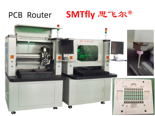
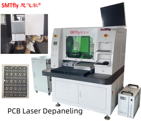
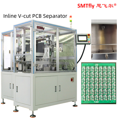
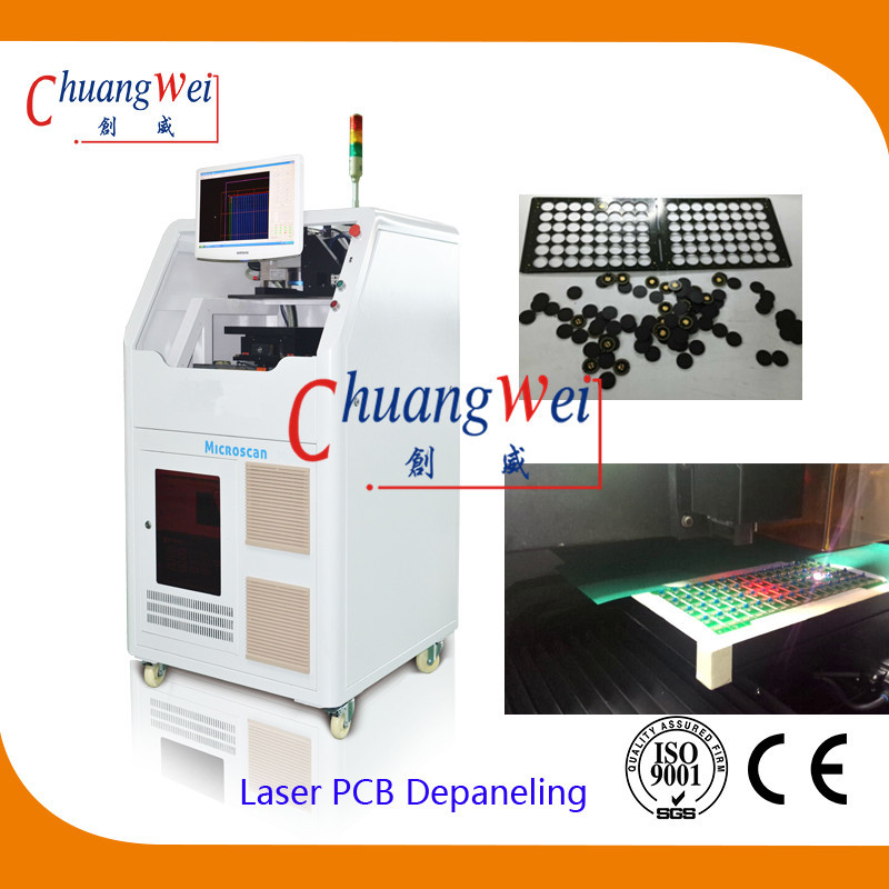
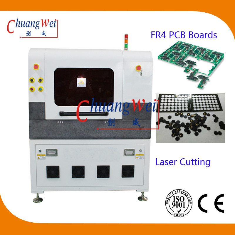
High Precision Pcb Depaneling Equipment All Solid State UV Laser 355nm Industrial PCB Laser Depaneling


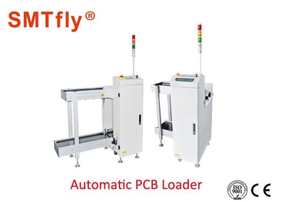
PCB depaneling (singulation) laser machines and systems have been gaining popularity over recent years. Mechanical depanaling/singulation is done with routing, die cutting, and dicing saw methods. However, as the boards get smaller, thinner, flexible, and more sophisticated, those methods produce even more exaggerated mechanical stress to the parts. Large boards with heavy substrates absorb these stresses better, while these methods used on ever-shrinking and complex boards can result in breakage. This brings lower throughput, along with the added costs of tooling and waste removal associated with mechanical methods.

Increasingly, flexible circuits are found in the PCB industry, and they also present challenges to the old methods. Delicate systems reside on these boards and non-laser methods struggle to cut them without damaging the sensitive circuitry. A non-contact depaneling method is required and lasers provide a highly precise way of singulation without any risk of harming them, regardless of substrate.


Challenges of Depaneling Routing


  • Damages and fractures to substrates and circuits due to mechanical stress
  • Damages to PCB due to accumulated debris
  • Constant need for new bits, custom dies, and blades
  • Lack of versatility – each new application requires ordering of custom tools, blades, and dies
  • Not good for high precision, multi-dimensional or complicated cuts
  • Not useful PCB depaneling/singulation smaller boards
  •  
  • Lasers, on the other hand, are gaining control of the PCB depaneling/singulation market due to higher precision, lower stress on the parts, and higher throughput. Laser depaneling can be applied to a variety of applications with a simple change in settings. There is no bit or blade sharpening, lead time reordering dies and parts, or cracked/broken edges due to torque on the substrate. Application of lasers in PCB depaneling is dynamic and a non-contact process.


Specification


Laser Q-Switched diode-pumped all solid-state UV laser
Laser Wavelength 355nm
Laser Power 10W/12W/15W/17W@30KHz
Positioning Precision of Worktable of Linear Motor ±2μm
Repetition Precision of Worktable of Linear Motor ±1μm
Effective Working Field 300mmX300mm(Customizable)
Laser Scanning Speed 2500mm/s (max)
Galvanometer Working Field Per One Process 40mmх40mm


 High Precision Pcb Depaneling Equipment  All Solid State UV Laser 355nm 0            High Precision Pcb Depaneling Equipment  All Solid State UV Laser 355nm 1

Prodotti raccomandati
Mettetevi in ​​contatto con noi
Persona di contatto : Eric Cao
Telefono : 86-13922521978
Fax : 86-769-82784046
Caratteri rimanenti(20/3000)